
PLD Series - Part 2 - External ZX81 Keyboard Interface GAL

This post chronicles the design, programming, and testing of an external keyboard interface for my TS-1000, using only a single ATF22V10C GAL IC (Generic Array Logic Integrated Circuit chip)! The same interface will work on a ZX81, and a similar principle can be utilized on an interface for the ZX Spectrum, TS-1500, and the TS-2068.
If you haven't already, you can read the very first blog post I ever published, and also part 1 of this series, "PLD Series - Part 1 - Programmed My First GAL" before reading this post, but it is not necessary. I have written about other projects since that first post, but this one connects the first post with my most recent adventures in designing and building a ZX81 external mechanical keyboard.
Inspiration From Community
I strongly encourage all my readers to get involved in your local Makerspace and/or a community of like minded people through web forums or sites like Meetup. There is only so much one can accomplish working alone, and even though there is a lot to be learned from the Internet, the interaction and inspiration (I like to use the term "Cross Pollination") one gets from sharing their journey with other people of similar interests is invaluable.
I received a dose of "Cross Pollination" during the 4/4/22 meeting of the Timex/Sinclair Online User Group (timestamp 01:23:30). The host, David Anderson, shared a schematic that he created on EasyEDA for an external keyboard interface circuit. He found the original schematic in a computer/electronics magazine article, but in the video David could not recall the actual source for his EasyEDA version of the schematic.
I reached out to David while writing this post, and he kindly sent me a link to the original article written by Joe Williamson, on page 9 of the September 1985 issue (Volume III, Number 9) of "SUM" (The Sinclair/Timex Users Magazine), preserved on the Internet Archive.
There are "mass quantities" (SNL "Coneheads" reference 🤣) of old periodicals to consume, including books, manuals, and software all faithfully preserved on the Internet Archive. If you haven't checked out the Internet Archive or the Wayback Machine yet, I highly recommend it!
I went back and studied the schematic from the meeting's YouTube video so I could learn how to interface an external keyboard (like the one I made in part 1 of this post) to a ZX81/TS-1000 computer without modifying the keyboard headers on the computers circuit board. I had already modified the keyboard headers on both my TS-1000 and my brother's ZX81 to fit my prototype mechanical keyboard in part 2 of this post.
By connecting to the expansion port, others could keep their computers original and unmodified. Also, having the external interface for an additional keyboard allows the original membrane keyboard to still function, and could be used for two-player games!
One Way to Interface an External Keyboard
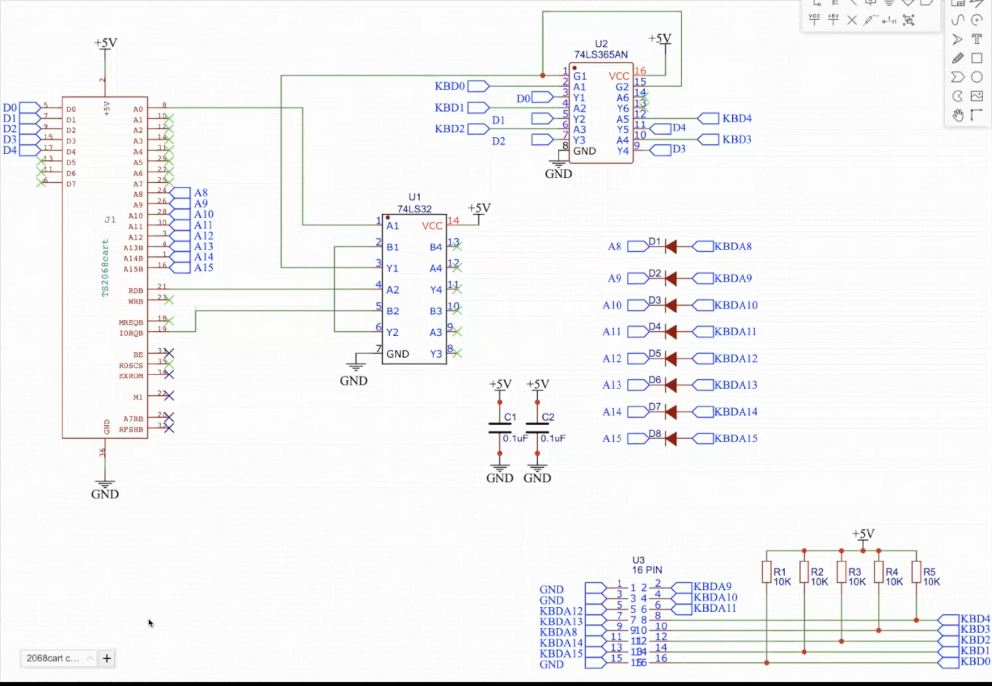
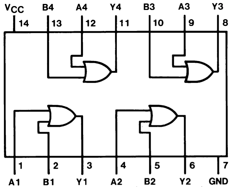
The original interface circuit uses two 74 series ICs. The first IC is a 74LS32, which basically contains four "OR" logic gates, each with two inputs, all on one chip.
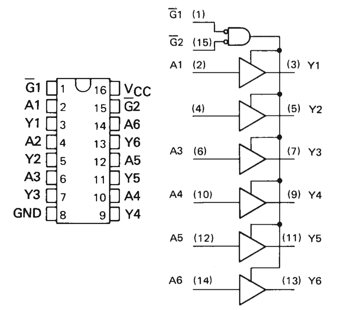
The second IC used is a 74LS365A, which contains six controllable output buffers (A.K.A "Bus Drivers") because with an IC like this, you could connect an external circuit to the data bus of a computer and have it set the data bus when the two control pins (/G1 on pin 1 & /G2 on pin 15, the forward slashes in each pin represents the bar over the top, and that means active low, or the complement) are logic "Low".
When I checked my inventory of 74 series ICs, (stored in a MySQL database on a cloud server 🤓) I saw that I had three 7432 ICs, but I knew even before checking that I didn't have any 74365 ICs.
Advantages of PLDs
Rather than being disappointed about not having any 74365 ICs in my parts inventory, I got excited...I now have a reason to use one of my GAL chips, and learn more about Programmable Logic Devices (PLDs)!
One of the advantages of using PLDs is that you do not always need to have a specific IC available, you can simply program a PLD to perform the functions of the IC you are replacing.
Another big advantage is rapid prototyping and development. You can create entire logic circuits, even state machines, on a PLD without any wiring or soldering. While in development/experimentation with PLDs, if the circuit needs to change, one only needs to change the configuration of the PLD in software.
Programming a GAL
As mentioned in part 1 of this series, one can use the free WinCUPL application offered by Microchip, or there is GALasm. I have GALasm installed on my MacBook Pro because I like working on the command line whenever possible 🤓.
In order to program a GAL, one ultimately needs a JEDEC file defining which of the GALs fuses should be blown by the programmer, and which should remain intact to create the logic desired. When using GALasm to produce a JEDEC file, one must start by creating a simple text file known as the PLD file. My preferred code editor is the free Visual Studio Code, and that is what I use to create my PLD files, but any text editor application will do.
GAL22V10 ; The device type
ext-kybd ; The signature

; Pin definitions:
;   1st line: Pins 1 - 12
;   2nd line: Pins 13 - 24

NC  NC  NC  NC  NC  NC  KBD4  KBD3  KBD2  KBD1  KBD0  GND
NC  D0  D1  D2  D3  D4  OE    NC    IORQ  RD    A0    VCC

; Logic equations

OE = /A0 * /RD * /IORQ

D0.T = KBD0
D0.E = OE
D1.T = KBD1
D1.E = OE
D2.T = KBD2
D2.E = OE
D3.T = KBD3
D3.E = OE
D4.T = KBD4
D4.E = OE

DESCRIPTION:
This file creates a five bit tri-state buffer:

    KBD0 ---|>--- D0
    KBD1 ---|>--- D1
    KBD2 ---|>--- D2
    KBD3 ---|>--- D3
    KBD4 ---|>--- D4


Each buffer is enabled by ANDing the complement of three active low inputs:

    A0 - Address bus bit 0
    RD - ReaD
IORQ - Input/Output ReQuestThe PLD file must begin with a GAL device type designation on the first line, which in this case is "GAL22V10" (GALasm doesn't recognize the ATF22V10C, but they are compatible enough). The second line of the PLD file is the eight byte long "signature", which is actually written into the GAL's signature.
Single line comments may be placed anywhere in a PLD file by preceding the comment with a semicolon. Comments are not interpreted by GALasm, but are helpful for us humans. GALasm also ignores extra whitespace (space, tab, & new line), which like comments, make PLD files easier to read.
PLD File Pin Definitions
The next two lines of the PLD file define the individual pin label names to be used in the logic equations to follow, or "NC" for "Not Connected". It is simply all pins in order from pin 1 to whatever the last pin is for the GAL being defined. Again, GALasm ignores whitespace, so the "new line" dividing the pin definitions is only for readability, thereby not having everything on one line, but that creates another problem. Having the pin definitions on two separate lines and in a "left-to-right" sequence of ascending order can create confusion when imagining the pins on a DIP IC package. DIP ICs have the numbering in ascending order starting at pin 1 going in one direction on that side of the DIP package, and then in ascending order in the opposite direction on the other side of the package.
The awkward order of the pin definitions, when picturing a DIP IC, is my reason for adding the two lines of comments before the definitions, all to prevent defining the pins incorrectly. Luckily, once GALasm is run on the PLD file, it generates a CHP file, a text file that depicts the pin definitions on a DIP package.
                                GAL22V10

                          -------\___/-------
                       NC |  1           24 | VCC
                          |                 |
                       NC |  2           23 | A0
                          |                 |
                       NC |  3           22 | RD
                          |                 |
                       NC |  4           21 | IORQ
                          |                 |
                       NC |  5           20 | NC
                          |                 |
                       NC |  6           19 | OE
                          |                 |
                     KBD4 |  7           18 | D4
                          |                 |
                     KBD3 |  8           17 | D3
                          |                 |
                     KBD2 |  9           16 | D2
                          |                 |
                     KBD1 | 10           15 | D1
                          |                 |
                     KBD0 | 11           14 | D0
                          |                 |
                      GND | 12           13 | NC
                          -------------------
The CHP file makes it much easier to visualize which inputs and outputs are programmed and with which signals, and for any retro computer geek like me, the text mode graphics of the CHP file bring back a lot of memories.
I couldn't find any documentation on what the rules/restrictions are on pin names in GALASM, so I did some digging into the source code, which is written in C, and saw the following:
- A name may begin with a forward slash to designate a complement/negation
- The size limit is eight characters (not including the leading forward slash if there is one)
- May contain any combination of letters and numbers
- May not be "AR" or "SP", as those are reserved for use in the logic equations for "Asynchronous Reset" & "Synchronous Preset" respectively
- "NC" must only be used to define unused pins
- "VCC" & "GND" must be defined and in the correct positions for the GAL specified on the first line of the PLD file
PLD File Logic Equations
On the ATF22V10C, just as on the original GAL22V10, pins 1 through 11 & pin 13 can only be configured as inputs, whereas pins 14 through 23 can be configured as either inputs or outputs. The designation in the name of 22V10 is that there are 22 pins that may be configured as inputs and only 10 that may be configured as outputs.
In order to define a logic equation:
- For simple outputs, start with the output pin name exactly as previously defined, or with a leading forward slash to indicate a complement/negation of the name. Start the equation with "AR" or "SP" when defining the Asynchronous Reset or Synchronous Preset respectively
- The output name must be followed by an equal sign
- Right hand terms of the equation are joined by "+", logical "OR", or "*", logical "AND" operators.
- The right hand side of the equation may contain any number of terms using combinations of input pin names and output pin names, both in uncomplemented or complemented form, so long as the number of terms does not exceed the limits of the defined output (each output of a GAL has a physical limit of terms. See the datasheet of your GAL)
Active Low Signals
Before explaining the first logic equation in the PLD file, and how it is derived from the original circuit, it would help to understand a staple of digital logic, the "Active Low" signal.
In digital logic, a signal that is considered to be "Active", or "True" when at a logic "Low" is called an "Active Low" signal. To anyone new to digital electronics this may seem contradictory. I know it made me scratch my head when first learning about it, since one might expect a logic "High", or binary 1, to always represent "True" or "On", and not the other way around. The truth of the matter is that "Active Low" signals are very common in digital logic design, and more often than not, signals going into and out of many common ICs are "Active Low" signals.
Defining The Enable Signal in the PLD File
The sole purpose of the 74LS32 IC in the original keyboard interface circuit is to combine all three of the signals, A0, RD, & IORQ into a single "Active Low Enable" signal by only using two of the four "OR" gates available. The single enable signal is fed to both G1 & G2 (both G1 & G2 have a line over the top, which means "the complement/negation of" in digital logic) of the 74LS365 bus driver IC.
Since we have a GAL, we only need to write one logic equation to replace the two "OR" gates of the 74LS32, but since the internal enable for the GAL's output pins needs to be "Active High", we need to "AND" the complements of the three "Active Low" inputs rather than "OR"ing the inputs, as was the case in the original circuit.
OE = /A0 * /RD * /IORQThe resulting logic equation is a practical application of "DeMorgan's Theorem", since we only want the Output Enable (OE) to be "Active High" when all three inputs are simultaneously logic "Low". We need the union of the complements.
Defining a Tri-State Output in a PLD File
In order to replace the need for the 74LS365, which contains six tri-state bus drivers (of which only five are used), five of the GALs outputs will need to be configured as tri-state outputs.
A tri-state output can be at a logic "Low", a logic "High", or at a high impedance, A.K.A. "High Z", which is like an open switch, or disconnected. The "High Z" state is important for avoiding "bus contention", which is when two or more devices on the same bus try to write values onto the bus at the same time. Imagine just one bit on an eight bit bus where one device wants to set that bit to a logic "High" while another device wants to reset the same bit to a logic "Low", that is a short circuit on that bit of the bus! ⚡️⚡️⚡️ The "High Z" state prevents the output from contending with any other devices on the bus until it is allowed to write to the bus via its OE signal. This is never a problem for multiple devices to read from the bus at the same time, only when more than one device tries to write to the bus at the same time.
For GALasm, an output is configured as a tri-state output by appending ".T" to the end of the output name. Also, when programming an output pin to be tri-state by appending the ".T" onto the pin name, a second output definition should follow with the same pin name but with a ".E" appended to it for "Enable". The "Enable" signal determines whether the output is "High Z" or not.
D0.T = KBD0
D0.E = OEThe two lines used per each tri-state output in the PLD file simply route each input pin to the tri-state output when OE is "True". So, whatever logic level exists at KBD0 will be present on the D0 output only when OE is "True", otherwise D0 will be "High Z" or disconnected from the data bus.
Programming The GAL
With the PLD file completed, I ran GALASM on the PLD file from the command line to have it create the JED file that will be used to program the GAL.
GALasm ./zx81-external-keyboard.pldIn addition, GALASM generates the CHP file mentioned earlier, a text file called the FUS file which shows the actual fuses that will be left intact and which ones will be blown, and lastly GALASM generates a PIN file, a text file showing the pin numbers in the first column, the names that were assigned by the PLD file for each pin, and that pin's type.
I then connected my TL866 II+ programmer to my MacBook Pro, inserted a blank ATF22V10C into it's Zero Insertion Force (ZIF) socket, and entered the following from the command line:
minipro -p ATF22V10C -w zx81-external-keyboard.jed -PTesting The GAL
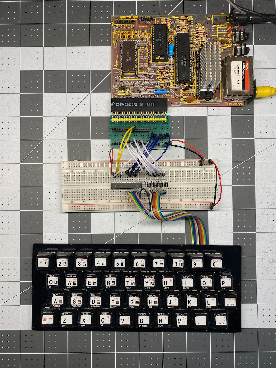
Before actually connecting the GAL to my TS-1000, I made a test circuit on a breadboard. I connected jumper wires to all the input pins, and LEDs to all the output pins.
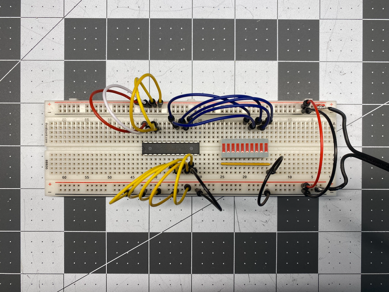
The test circuit confirmed that the bits that I set at the input pins only appeared on the outputs when all three of the inputs determining OE were simultaneously low. Having confidence in the programming of the GAL, it was time to connect it to my TS-1000 via a breadboard and my DIY breakout board from my latest post.

The breadboard only needed five 10k Ohm pull up resistors and eight diodes for the the address lines coming from the TS-1000. The jumper wires from my prototyping board then connect the breadboard and keyboard to the TS-1000.
IT WORKED RIGHT AWAY!!! It's rare that there isn't a missing wire, or a wire connected to the wrong pin somewhere. I hope this post inspires others to tinker and enjoy learning more about the technology that we use everyday.