
ZX81/TIMEX-SINCLAIR 1000 Custom Mechanical Keyboard Prototype - Part 3

In this third post in the series, the mechanical keyboard gets updated from wired switches on a laser cut acrylic plate to an actual printed circuit board (PCB), and not just switches soldered directly to the PCB, but a hot-swappable mechanical keyboard! How many kids on your street have hot swappable mechanical keyboards for their ZX81 retro computers? 🤓
It Started With A Hand Wired Prototype
It has been over a year since I published Part 2 of this series, and now in conjunction with my brother & our work on the Kilo-Zed case, the time has come to finally take the mechanical keyboard to a new level. I have always wanted to design a custom PCB with a computer aided design (CAD) program and then have them professionally made, and this keyboard PCB is my first attempt at doing just that.
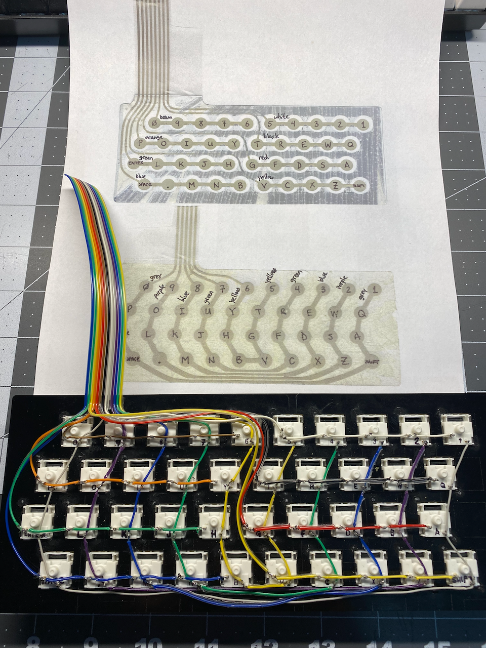
In the previous incarnation of the ZX81/TS-1000 mechanical keyboard, chronicled in Part 1 & Part 2 of this series, I used the laser cutter at my makerspace, the Tech Valley Center of Gravity, to cut a 3mm thick piece of black acrylic to make a switch mounting plate. Since there was no PCB then, I hand soldered rainbow colored ribbon cable in a way to form all of the rows and columns that make up the keyboard matrix.
The hand wired keyboard was a fun project, and as a prototype/proof of concept I would call it a success, but having a printed circuit board makes it easier to share the fun with others. Printed circuit boards are also self contained, more reliable, easier to build, and the only way to get a consistent repeatable product. As you will see later in this post, unlike hard wired switches, the PCB gets us closer to making it possible to have the keyboard hot-swappable!
Designing A Custom PCB
The first step to making a custom PCB is to get the circuit represented somewhere in the form of a schematic. A schematic is a graphical representation of the components and connections that make up an electric circuit. There was a time when schematics were hand drawn, but for quite some time now there are computer programs, and even web sites, that make drawing and designing electrical schematics much easier.
The nice thing about using a computer to design electrical/electronic circuits is that many programs can assist in simulating your circuit, test for errors in your design, and lastly allow you to take the design straight to a physical PCB model.
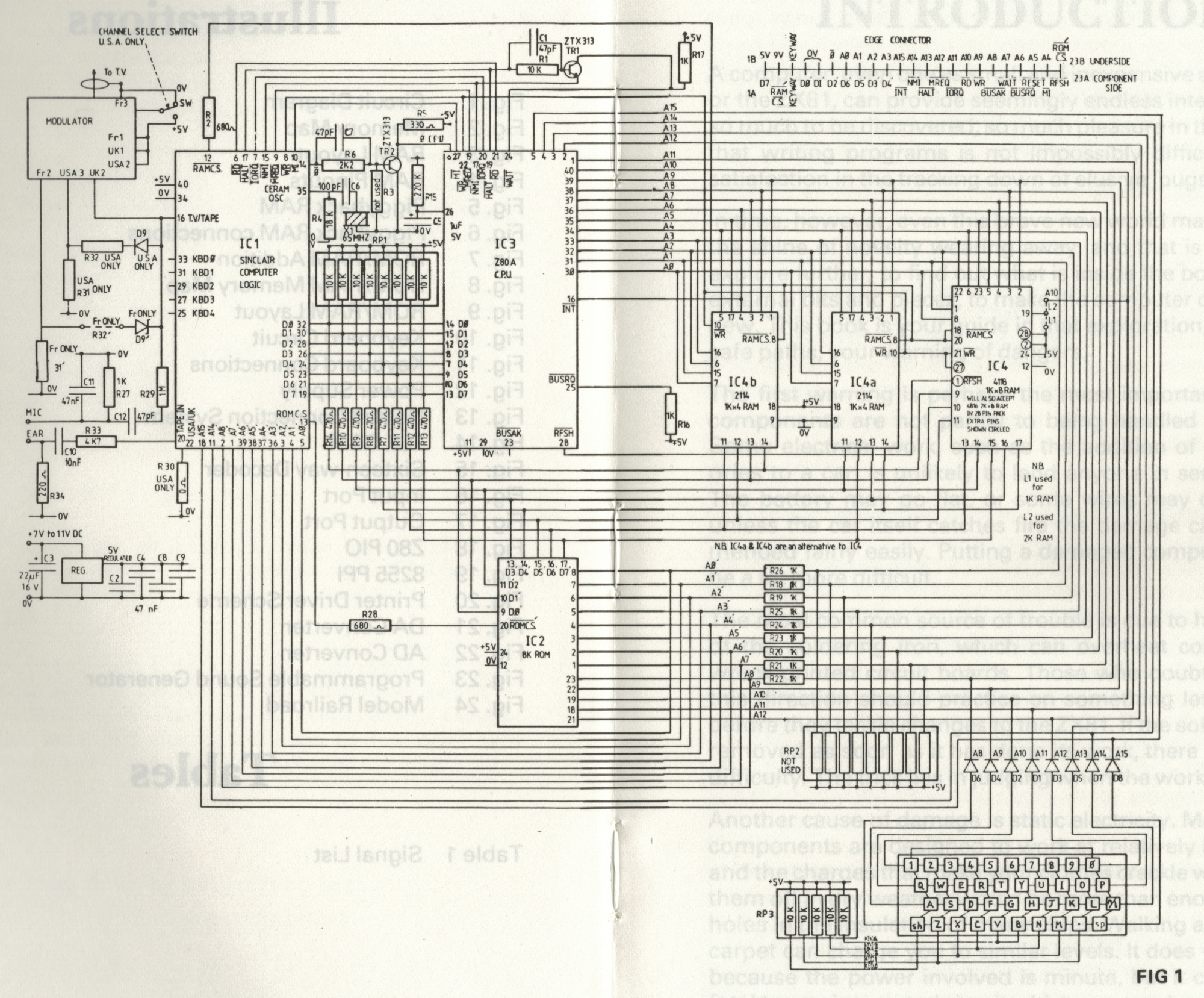
Since the design of the circuit has already been taken care of by Sir Clive Sinclair's engineers back in the late 70's - early 80's, I would only need to duplicate the keyboard switch matrix (shown in the bottom right corner of the ZX81 schematic above) into a CAD program of my choosing.
Free & Open Source KiCAD
For a few years now, I have been using KiCAD, as per their web site, "A Cross Platform and Open Source Electronics Design Automation Suite". I have heard the name pronounced two different ways by others in YouTube videos, but according to an article on Wikipedia the name is pronounced /ˈkiːˌkæd/KEE-kad. There is also a very popular on-line electronic design automation (EDA) application known as EasyEDA, and it has a very similar interface. One of the major differences is of course that in order to use EasyEDA, one needs an Internet connection, whereas KiCAD runs natively on your computer. KiCAD is multi-platform and will run on Linux, Mac OSX, & Microsoft Windows.
As mentioned earlier, the first step to make a PCB in an EDA application is to first get a schematic entered, so I created a new project in KiCAD and started adding all forty key switches and the two headers for connecting the keyboard to the computer.
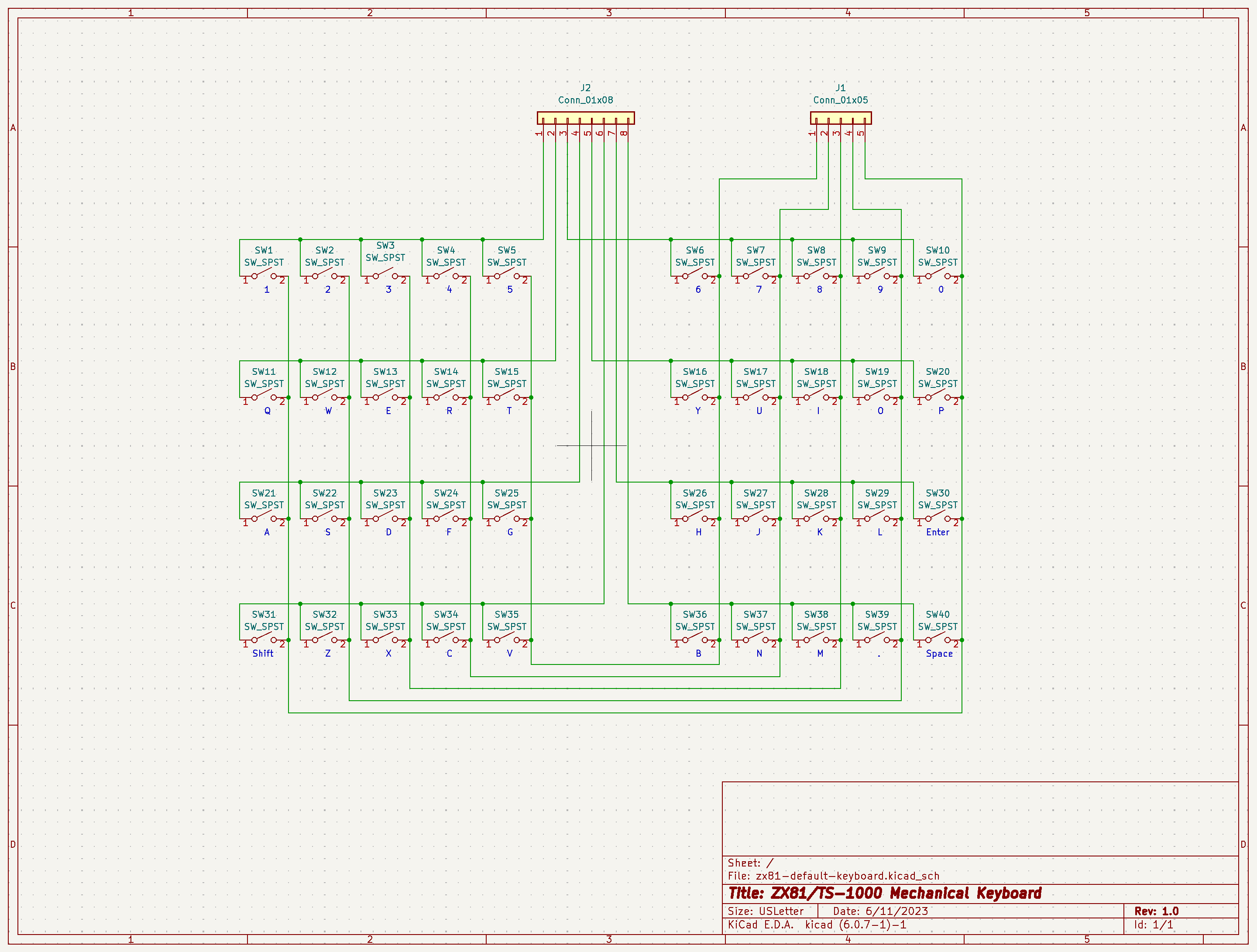
Once the schematic has been created and saved in KiCAD's Schematic Editor, and as long as the schematic symbols have footprint files linked to them, work can resume in KiCAD's PCB Editor. Footprint files are physical representations of components that need to co-exist on the PCB. For example, each switch in the schematic has a footprint file associated with it so that when going over to the PCB Editor it will know that there are forty switches with a given size and hole placement. KiCAD comes with many libraries of symbols and footprints for practically every electronics component in existence, but if needed/desired a user may also create custom symbols and footprints.
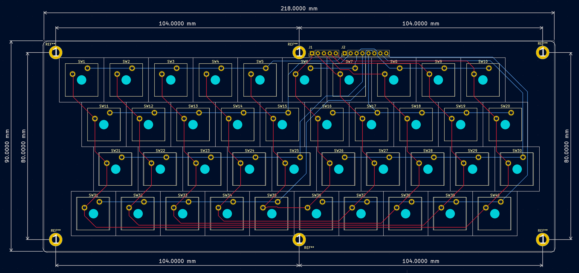
When first going to the PCB Editor from the schematic all of the components are just dropped onto the screen with thin light colored lines showing the connections between components from the schematic. The user can rearrange the components physically on the screen and draw an outline of the actual PCB with it's dimensions.
In my particular case, I had to make sure that the spacing of the key switch footprints coincided with the layout of the ZX81 keyboard. Luckily, KiCAD's PCB Editor has a layer named "User.Drawings" which I used to place an SVG of the laser cut switch plate that I generated on swillkb's Plate & Case Builder site. With the plate SVG as a guide, and after setting the grid size in the PCB Editor, I was able to get all of the switches arranged in a way to be true to the layout of the ZX81 keyboard.
Lastly, once the PCB's outline is drawn and all of the components are placed on the PCB, the user can draw the actual copper traces that connect the components into the circuit. This is where the thin light colored lines are very helpful, as one can immediately see when something is not yet connected, or when a trace needs to be re-routed to avoid crossing another trace. I went through several iterations in moving the two connection headers around, and cleaning up the routing of the copper traces to make it consistent and organized looking. Going through the steps to position everything several times made me more skilled at working with the user interface, and things that at first seemed awkward and counterintuitive now make sense and feed more natural.
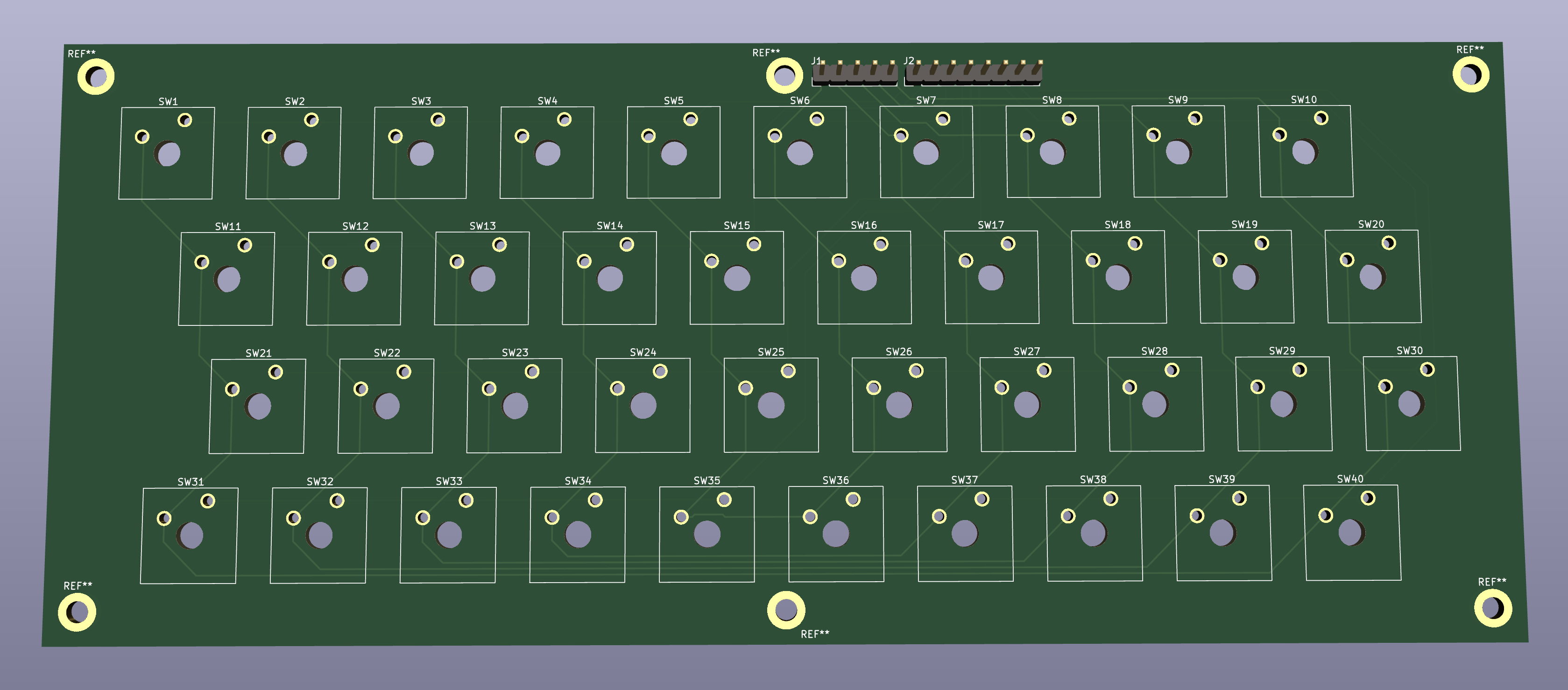
The final keyboard PCB design resulted in a two sided PCB with the top circuit traces displaying in red and the bottom side circuit traces displaying in blue in the screenshot above. During the PCB layout process, I was able to switch into a very convenient 3D Viewer, which was very nice to help in visualizing what the final product might end up looking like while moving things around.
Generating & Sending The Gerber Files To JLCPCB
This post is not sponsored by JLCPCB, a manufacturing house in The People's Republic of China. I am mentioning them as they were the first company that I have used to manufacture PCBs for me. The choice to use JLCPCB wasn't based on any specific reason or review. There are several PCB manufacturing companies out there, and I may try others in the future to compare services, but I imagine they are all going to be fairly similar.
Once the PCB was finished in KiCAD I went to the JLCPCB web site and worked my way through the steps to get a quote/order together. For the size and type of parameters that I selected, there was a minimum quantity of five boards, and a variety of shipping options with DHL. I placed my order on June 20th and soon after placing my order, I received a message from the free review service at JLCPCB that my order had some technical issues. It turned out that I was missing the drilling file as well as the top & bottom solder mask files when I uploaded all of the Gerber files that were generated in KiCAD...rookie mistake.
Soon after uploading a new zip archive of all of the required Gerber files to JLCPCB, I was able to view the progress of my order in real time. On June 23rd my PCBs were finished and awaiting DHL to pick them up for delivery, and on June 26th my first professionally manufactured prototype PCBs arrived at my home.
I feel it is important to recognize and appreciate the significance of how amazing it is to go from a computer design to an extremely professional quality PCB in less than a week!
FreeCAD Switch Mounting Plate Design
Now that I had a gorgeous PCB to replace the hand wired laser cut switch plate, it was time to design a prototype key switch mounting plate. The key switches that I am using, and which are the most common standard these days, were designed by a German company, CherryMX. I don't currently own any actual CherryMX key switches, rather an alternative made Gateron, a Chinese manufacturer. The Gateron switches are built to the CherryMX standard dimensions, and both come in fundamentally two mounting possibilities: 3 pin or 5 pin mounting.
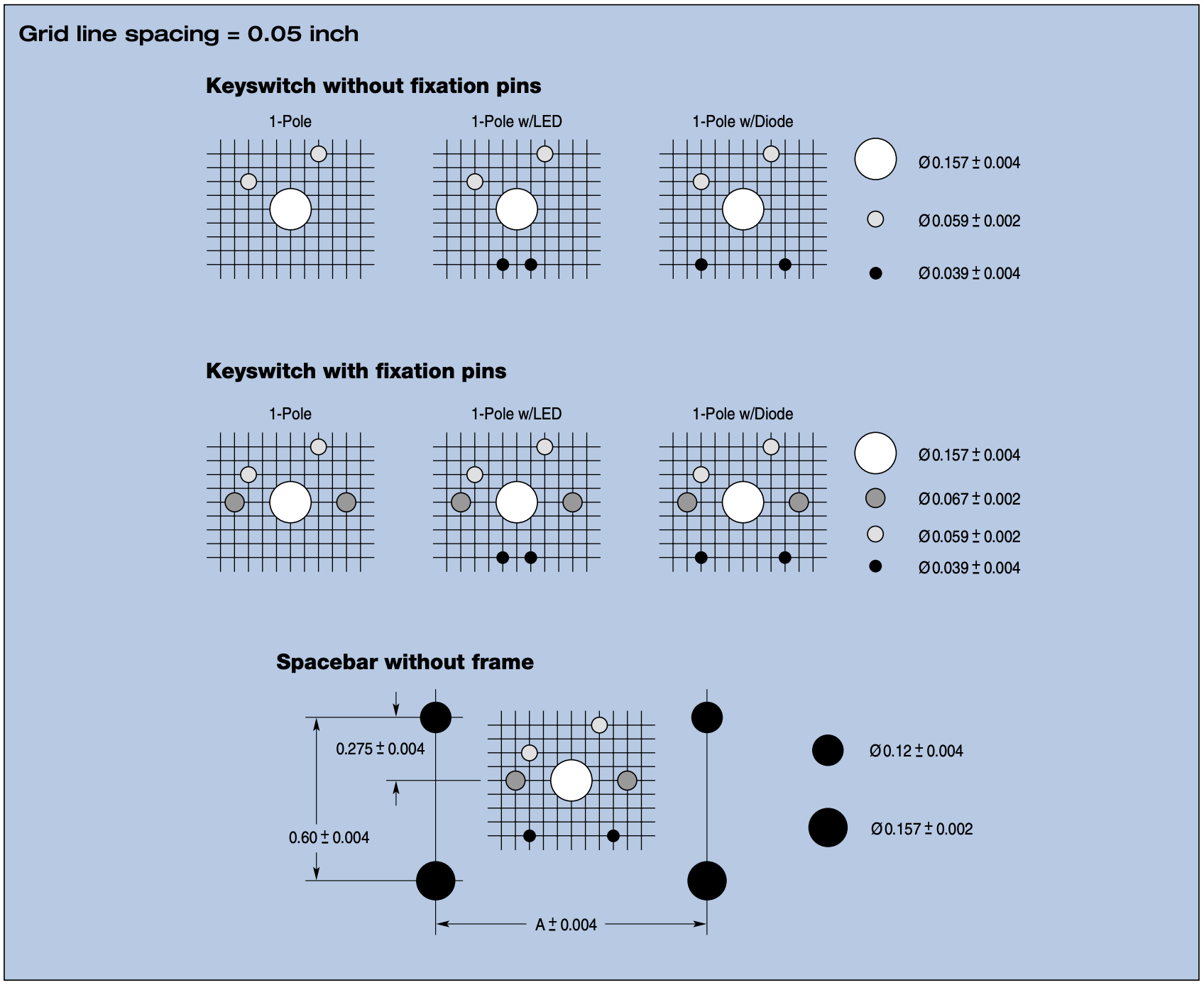
The 3 pin mounting style is intended to be mounted with a mounting plate to mechanically stabilize the switches, whereas the 5 pin style switches offer additional mechanical stability by adding two additional plastic pins to go into the PCB for a total of three mounting pins and two electrical connection pins. The switches that I have for the ZX81 mechanical keyboard are the 3 pin variety (shown in the top left of the specification sheet above, "keyswitch without fixation pins").
I created a new file in FreeCAD, a multiplatform, free, and open source CAD program, and imported a step file of the PCB that I exported from KiCAD into the new FreeCAD file. I am still learning how to use FreeCAD, and spent a lot of time beating my head against the wall trying to get a working 3D model of the key switch plate built on top of the step file model of the PCB. 🤬
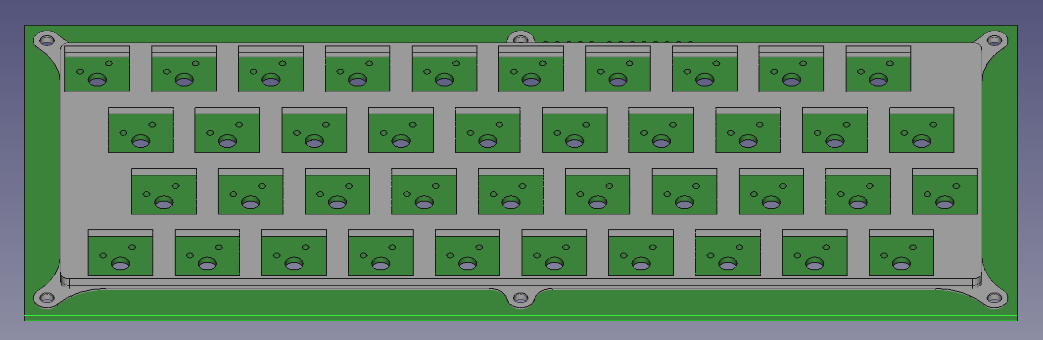
FreeCAD has a STEEP learning curve, but I believe in open source and would like to see it thrive and prosper, so I suffered through the frustrations and failures. Needless to say, once I was able to search the forums and YouTube videos, I ended up with a working model for a prototype switch mounting plate which I promptly sent to my slicing program, Ultimaker Cura, for 3D printing.
Normally when I export an STL file from FreeCAD and open it in Ultimaker Cura everything goes smoothly, buy apparently I still had another chunk of learning curve ahead of me! When I previewed the model in Cura, I was seeing a layer covering the openings of the switch plate where the key switches are supposed to be inserted in, but that layer wasn't visible when looking at the model. I did some searching online and the first forum posts that I read hinted towards a setting in Cura under the "Mesh Fixes" settings, a setting called "Remove All Holes", which when checked/enabled would do what I was observing. I thought, "that's got to be the problem", but when I checked that setting in Cura it was disabled.
Once I finally figured out the issue, everything worked as it should, and I decided to make a short video and share it on YouTube in the hopes of helping someone else experiencing the same or similar problem.
Making The Keyboard Hot Swappable!
For those who aren't already aware of the mechanical keyboard craze amongst software developers and gamers, and what it means to have a hot-swappable keyboard, it means that the switches of the keyboard can be individually swapped out with different switch types. There are a variety of switches that have a different sound and/or tactile feel to them, basically providing something for just about everyone's preferences. So having a keyboard that accommodates the replacement of individual switches without requiring a soldering iron is having your cake and eating it with any utensil you want...bare hands, fork, spoon, or chop sticks!
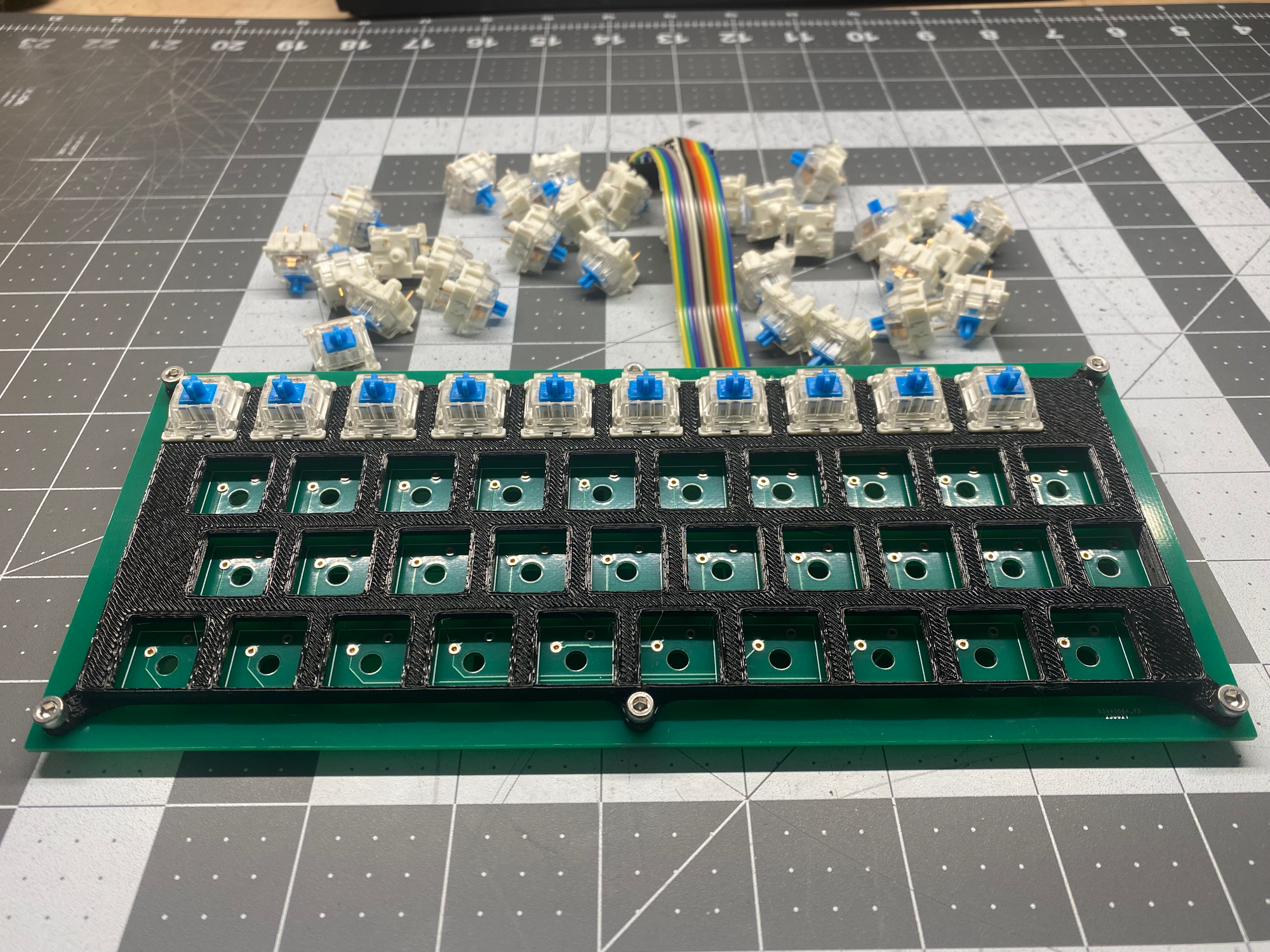
The key to making a PCB hot-swappable is by soldering in Mill-Max receptacles into the solder pads of the PCB where you would normally solder in the contacts of the key switches. Mill-Max makes a large range of sockets and connectors, and for my needs it was the 3305-0-15, of which I ordered 170 from Digikey.
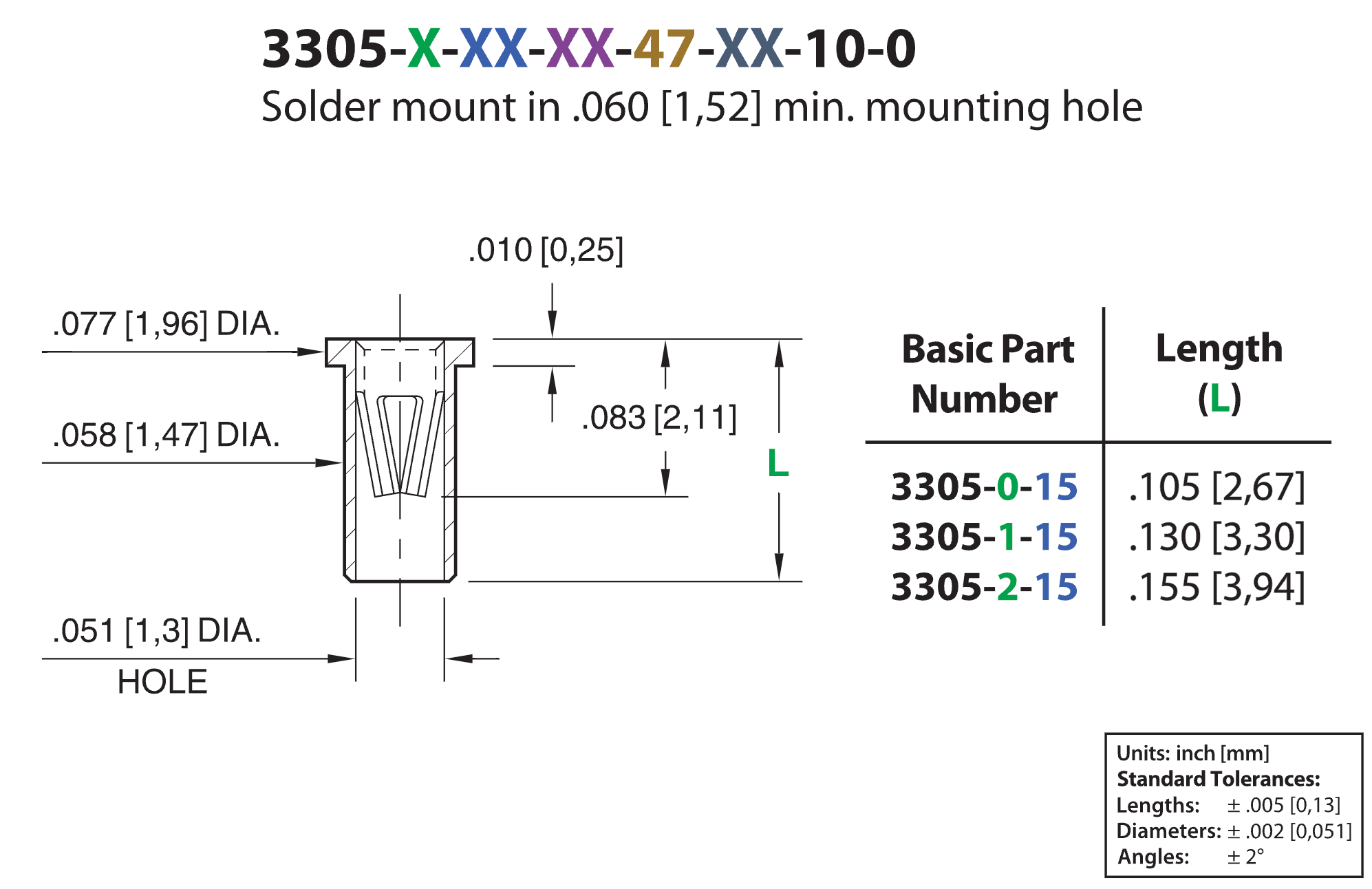
The receptacles arrived the day before writing this blog post, and I didn't waste any time to start the assembly process. My eyesight isn't what it used to be, so I needed magnifier glasses and tweezers to get the 80 receptacles into the solder pads one at a time.
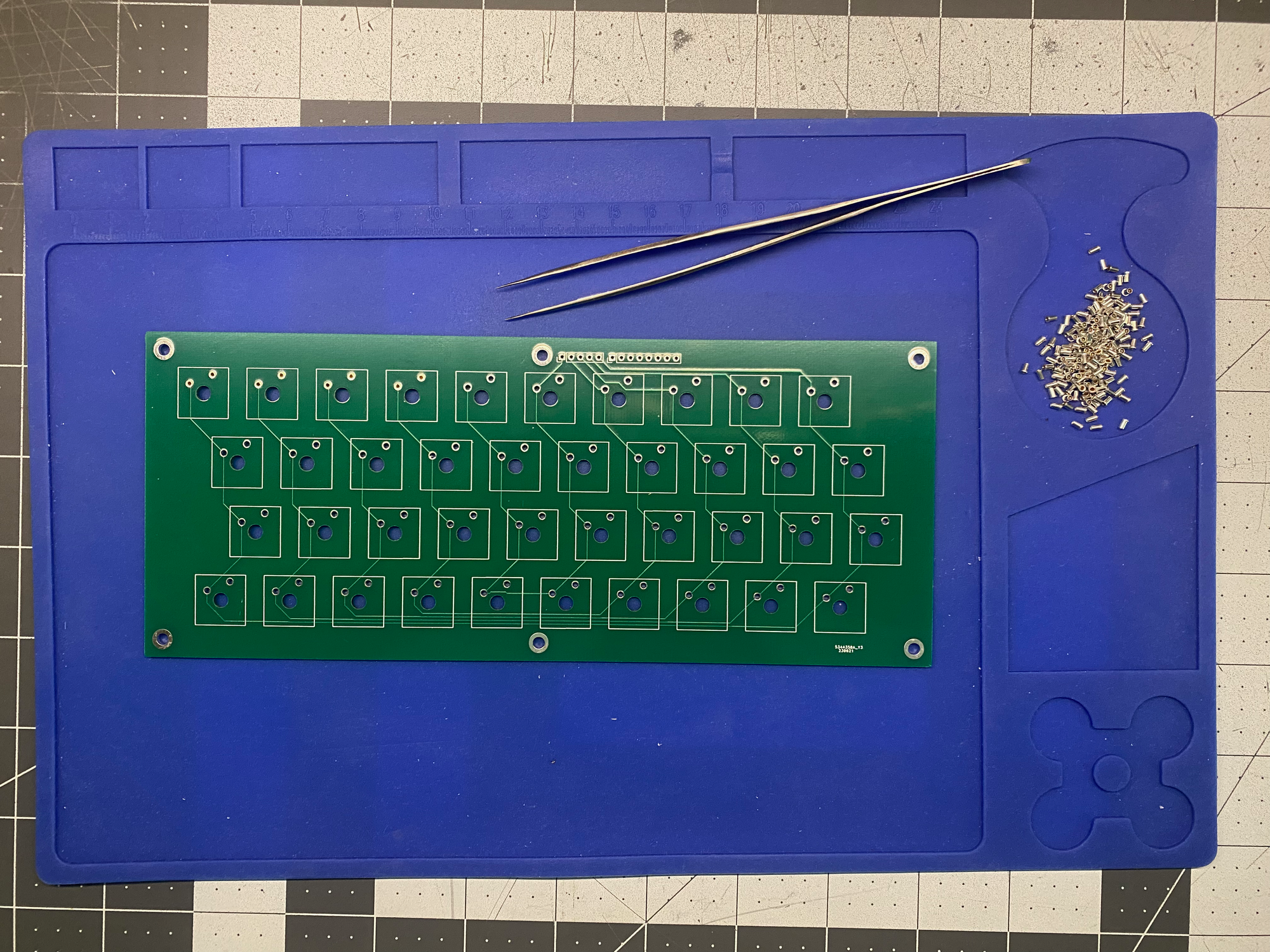
Some of the receptacles required a bit of force to get them in, but by using the flat end of the tweezers I was able to apply steady, even pressure with my fingers to press the receptacles all the way into the holes and flush with the top of the solder pads.
Attaching The Ribbon Cable
I was so excited to start pressing in the Mill-Max receptacles that I got ahead of myself...I hadn't even electrically tested my PCBs on the ZX81 to make sure that I didn't make a mistake when sending the file to JLCPCB! 🤣 So, rather than installing all of the receptacles, I stopped before finishing the top row of switches and started making up the ribbon cable with the DuPont connectors.
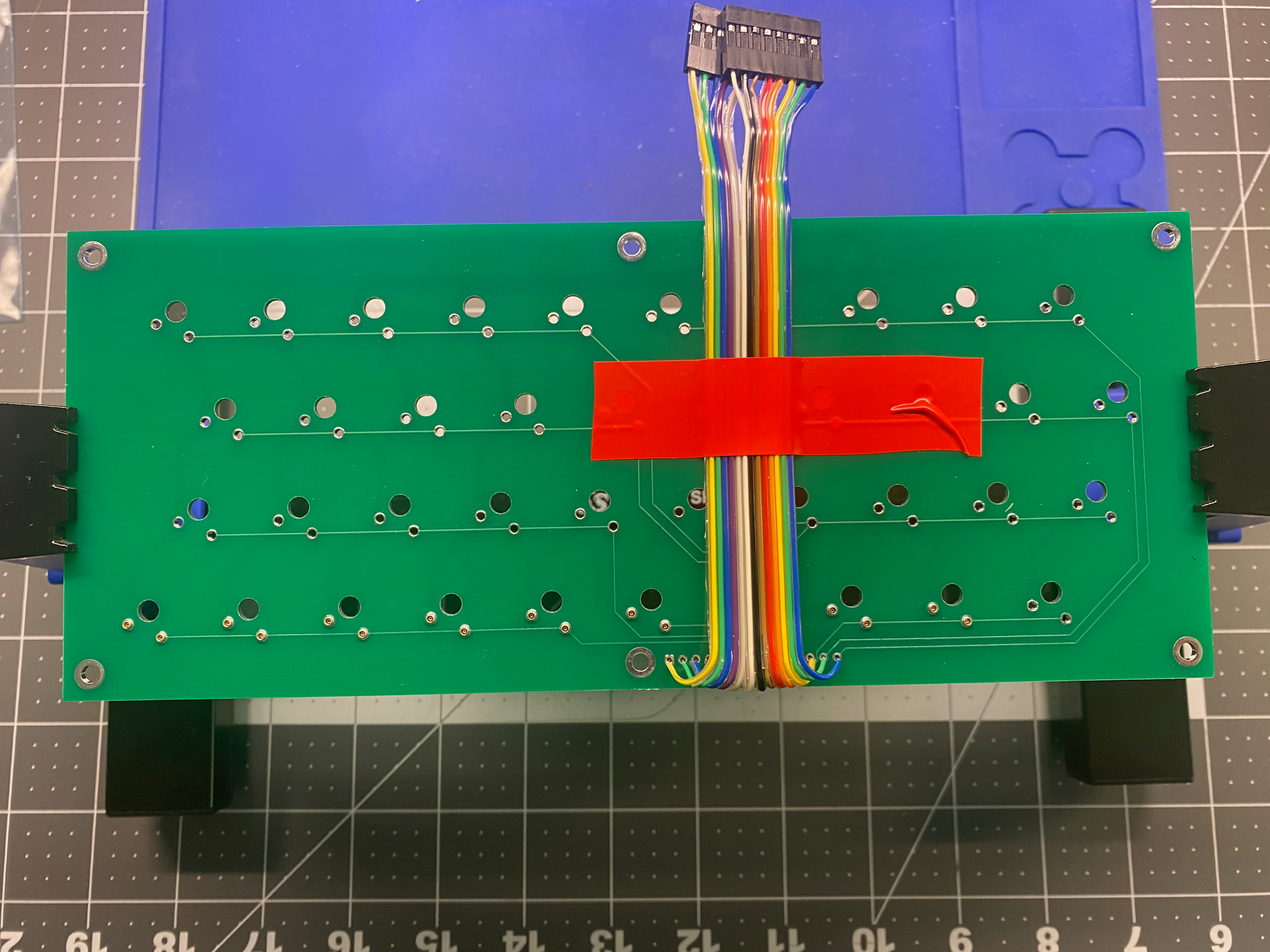
I connected the keyboard PCB to my brother's ZX81, powered it up, and with the tweezers systematically went through each switch position and shorted the solder pads together and observed the monitor to make sure that the ZX81 was registering the correct key press, which much to my happiness all worked correctly and I didn't have to cut traces and solder in any bodge wires (wires soldered in for a correction or update to a PCB).
With the keyboard properly tested, I continued pressing in the remaining receptacles. The next step was to tape the top side of the PCB with Kapton thermal tape, because even though almost all of the receptacles were pressed in tightly, a YouTube video I watched a few days prior to my build recommended taping the top side with Kapton tape to prevent the receptacles from moving or falling out during soldering.
Assembling The PCB & The Mounting Plate
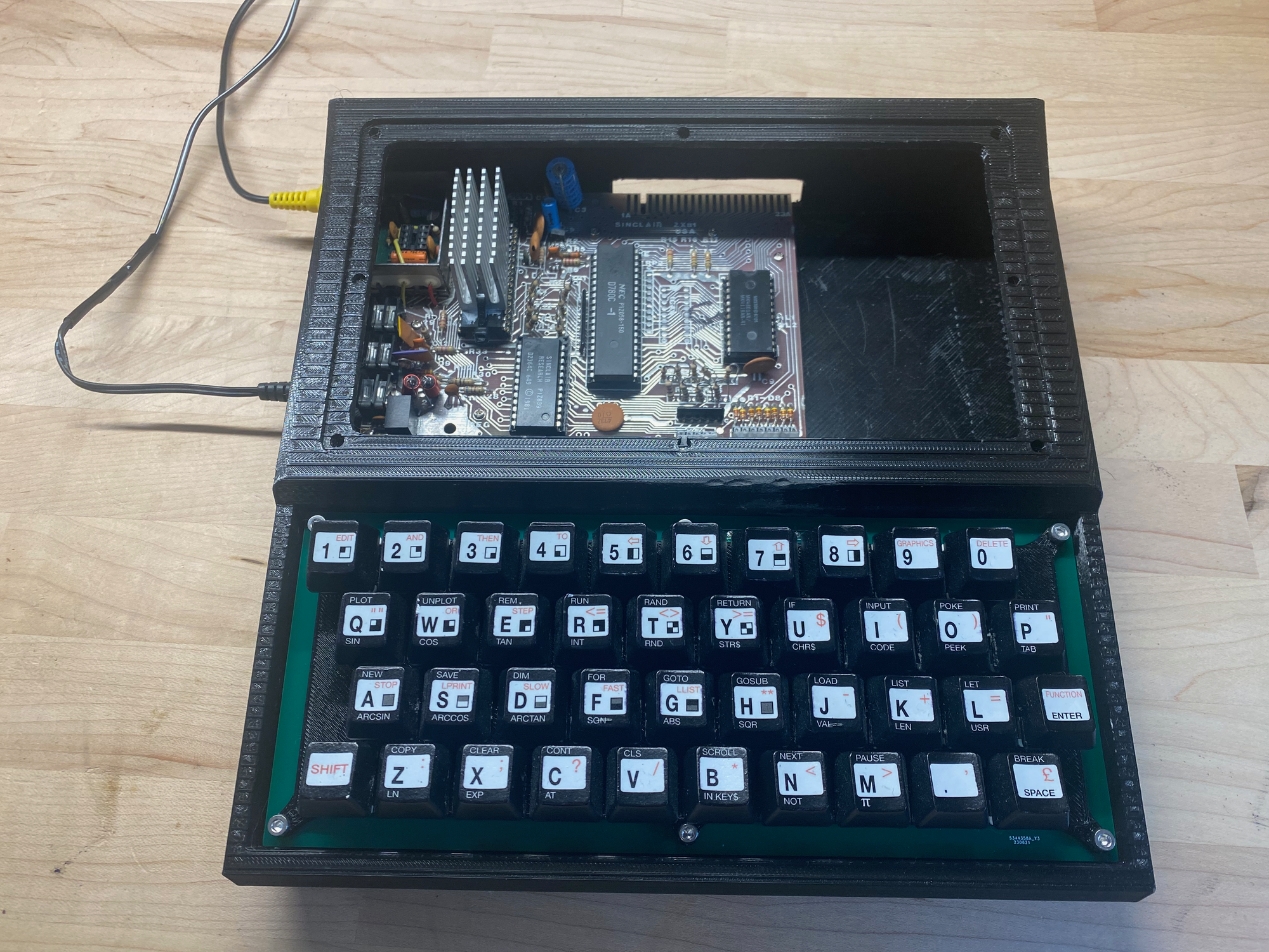
While I was soldering all of the receptacles to the PCB, my 3D printer was finishing up printing the mounting plate. I separated the mounting plate from the build plate of the printer, and then separated the mounting plate from the sacrificial raft, and after a minor clean up with a hobby knife, it was the moment of truth! The mounting plate fit perfectly, I couldn't be happier after all of the struggling with my learning curve. Even though the end goal is to mount this keyboard directly into the bottom half of the Kilo-Zed computer case, I decided to assemble the PCB and the mounting plate with 3mm stainless steel screws, washers, and nuts.

Next, I installed 40 Gateron Blue key switches, and then transferred the custom key caps I made using blank black key caps and water transfer decals that I designed myself in Inkscape.
I have already sent my brother the dimensions for the six mounting screws on the PCB so that he can add mounting stand offs to the bottom half of the version 3.0 Kilo-Zed case. Also, I just ordered some Lubed Akko/Gateron Yellow key switches to try them out in contrast to the "clicky" Gateron Blue switches. The yellow switches are supposed to feel softer and are also supposed to be quieter. Now that the keyboard PCB is hot-swappable, I will be able to easily switch some or all keys to different switches whenever I want.